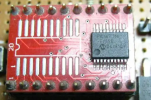
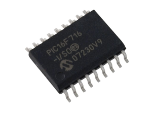
The PIC16F716 is a specialized 8-bit microcontroller ( MCU ) celebrated for its hardened PWM module and 28-pin compact architecture, featuring 3.5KB of flashprogram memory and 128 bytes of EEPROM. Unlike general-purpose chips, this microprocessor is deeply embedded in closed-loop motor controls, brushless DC fans, automotive power windows, and industrial solenoid drivers. Its protected status often relies on locked configuration bits that prevent external readout of the binaryfile. However, when the original source code is lost after a decade of service, or when a malfunctioning unit needs security auditing, the legitimate owner faces a barrier: the securedmemory holds calibration maps and timing loops that cannot be recreated from scratch. To extractICcode legally is not an act of theft—it is an act of system restore and preservation.
Thách thức khi cố gắng mở khóa vi điều khiển Microchip PIC16F716 nằm ở thiết kế bảo vệ nhiều lớp của nó. Các lệnh đọc đơn giản chỉ trả về số 0 vì bit được bảo mật kích hoạt tường lửa bộ nhớ phần cứng của vi xử lý Microchip PIC16F716. Phương pháp đảo ngược kỹ thuật của chúng tôi bắt đầu bằng việc gây nhiễu cấp thấp để tạm thời vô hiệu hóa lớp bảo vệ này, cho phép chúng tôi trích xuất nội dung thập lục phân thô từ các vùng flash và EEPROM của vi điều khiển Microchip PIC16F716. Không giống như các chip chỉ có flash, kho lưu trữ EEPROM thường lưu trữ ID thiết bị duy nhất và các giá trị hiệu chỉnh—mất chúng có nghĩa là mất hiệu chuẩn trường. Sau đó, chúng tôi khôi phục phần mềm vào một tệp nhị phân được sắp xếp của vi điều khiển Microchip PIC16F716, bảo toàn các vectơ ngắt và từ cấu hình. Mục tiêu là khôi phục mọi byte dữ liệu mà không làm hỏng các phân đoạn vi xử lý Microchip PIC16F716 được bảo vệ. Quá trình này đòi hỏi sự kiên nhẫn, vì vi điều khiển Microchip PIC16F716 sẽ tự hủy nếu bị dò tìm không chính xác; Chúng tôi không tiết lộ toàn bộ phương pháp tấn công, nhưng chúng tôi đảm bảo trích xuất dữ liệu sạch sẽ mà vẫn giữ nguyên bộ nhớ của chip Microchip PIC16F716 để có thể sao chép trong tương lai.
The PIC16F7X devices have a 13-bit program counter capable of addressing an 8K word x 14-bit program memory space. The PIC16F716 devices have 8K words of FLASH program memory and the PIC16F716 devices have 4K words. The program memory maps for PIC16F7X devices are shown in Figure 2-1. Accessing a location above the physically implemented address will cause a wraparound.
एक लॉक किए गए माइक्रोचिप PIC16F716 MCU को खोलने की कोशिश करने की चुनौती इसके स्तरित सुरक्षात्मक डिजाइन में निहित है। सरल रीड कमांड केवल शून्य लौटाते हैं क्योंकि सुरक्षित बिट माइक्रोचिप PIC16F716 माइक्रोप्रोसेसर हार्डवेयर मेमोरी फ़ायरवॉल को ट्रिगर करता है। हमारा रिवर्स इंजीनियरिंग दृष्टिकोण इस गार्ड को अस्थायी रूप से निलंबित करने के लिए निम्न-स्तरीय गड़बड़ के साथ शुरू होता है, जिससे हम माइक्रोचिप PIC16F716 माइक्रोकंट्रोलर के फ्लैश और EEPROM क्षेत्रों से कच्चे हेक्सिमल सामग्री को डंप कर सकते हैं। फ्लैश-ओनली चिप्स के विपरीत, EEPROM अभिलेखागार अक्सर विशिष्ट डिवाइस आईडी और ट्रिमिंग मानों को संग्रहीत करता है – उन्हें खोने का मतलब है फ़ील्ड कैलिब्रेशन खोना। फिर हम फर्मवेयर को माइक्रोचिप PIC16F716 MCU की एक संगठित बाइनरी फ़ाइल में पुनर्स्थापित करते हैं, हम हैक करने का पूरा तरीका नहीं बताते, लेकिन हम एक साफ़ एक्सट्रैक्ट की गारंटी देते हैं जो माइक्रोचिप PIC16F716 चिप की मेमोरी को भविष्य में डुप्लीकेशन के लिए सही-सलामत रखता है।
Сложность попытки взлома заблокированного микроконтроллера Microchip PIC16F716 заключается в его многоуровневой защитной конструкции. Простые команды чтения возвращают только нули, поскольку защищенный бит активирует аппаратный брандмауэр памяти микропроцессора Microchip PIC16F716. Наш подход к реверс-инжинирингу начинается с низкоуровневого глитчинга для временной приостановки этой защиты, что позволяет нам получить необработанное шестнадцатеричное содержимое из областей флэш-памяти и EEPROM микроконтроллера Microchip PIC16F716. В отличие от микросхем, содержащих только флэш-память, архив EEPROM часто хранит уникальные идентификаторы устройств и значения подстройки — их потеря означает потерю полевой калибровки. Затем мы восстанавливаем прошивку в организованный двоичный файл микроконтроллера Microchip PIC16F716, сохраняя векторы прерываний и слова конфигурации. Цель состоит в том, чтобы восстановить каждый байт данных без повреждения защищенных сегментов микропроцессора Microchip PIC16F716. Этот процесс требует терпения, поскольку микроконтроллер Microchip PIC16F716 самоуничтожится при неправильном зондировании; Мы не раскрываем полную методику взлома, но гарантируем чистое извлечение данных, которое сохранит память микросхемы Microchip PIC16F716 в целости и сохранности для дальнейшего копирования.
The RESET Vector is at 0000h and the Interrupt Vector is at 0004h. The Data Memory is partitioned into multiple banks, which contain the General Purpose Registers and the Special Function Registers. Bits RP1 (STATUS<6>) and RP0 (STATUS<5>) are the bank select bits: Each bank extends up to 7Fh (128 bytes). The lower locations of each bank are reserved for the Special Function Registers. Above the Special Function Registers are General Purpose Registers, implemented as static RAM. All implemented banks contain Special Function Registers.
لاک مائیکروچپ PIC16F716 MCU کو کھولنے کی کوشش کرنے کا چیلنج اس کے پرتوں والے حفاظتی ڈیزائن میں ہے۔ سادہ پڑھنے والی کمانڈز صرف صفر واپس کرتی ہیں کیونکہ محفوظ بٹ مائکروچپ PIC16F716 مائکرو پروسیسر ہارڈویئر میموری فائر وال کو متحرک کرتا ہے۔ ہمارا ریورس انجینئرنگ اپروچ اس گارڈ کو عارضی طور پر معطل کرنے کے لیے کم سطح کی گڑبڑ سے شروع ہوتا ہے، جس سے ہم مائیکروچپ PIC16F716 مائیکرو کنٹرولر کے فلیش اور EEPROM علاقوں سے خام ہیکسیمل مواد کو پھینک سکتے ہیں۔ صرف فلیش چپس کے برعکس، EEPROM آرکائیو اکثر منفرد ڈیوائس آئی ڈیز اور ٹرمنگ ویلیوز کو اسٹور کرتا ہے — ان کو کھونے کا مطلب فیلڈ کیلیبریشن کو کھونا ہے۔ اس کے بعد ہم فرم ویئر کو مائیکرو چِپ PIC16F716 MCU کی ایک منظم بائنری فائل میں بحال کرتے ہیں، جو انٹرپٹ ویکٹرز اور کنفیگریشن الفاظ کو محفوظ رکھتے ہیں۔ مقصد محفوظ مائیکرو چِپ PIC16F716 مائیکرو پروسیسر سیگمنٹس کو خراب کیے بغیر ہر ڈیٹا بائٹ کو بازیافت کرنا ہے۔ اس عمل کو صبر کی ضرورت ہے، کیونکہ اگر غلط طریقے سے جانچ پڑتال کی گئی تو مائکروچپ PIC16F716 مائیکرو کنٹرولر خود کو تباہ کر دے گا۔ ہم مکمل ہیک طریقہ کار کو ظاہر نہیں کرتے ہیں، لیکن ہم ایک صاف نچوڑ کی ضمانت دیتے ہیں جو مستقبل میں نقل کے لیے مائکروچپ PIC16F716 چپ کی میموری کو برقرار رکھتا ہے۔
Some frequently used Special Function Registers from one bank may be mirrored in another bank for code reduction and quicker access. The register file (shown in Figure 2-2 and Figure 2-3) can be accessed either directly, or indirectly, through the File Select Register FSR. The Special Function Registers are registers used by the CPU and peripheral modules for controlling the desired operation of the device. These registers are implemented as static RAM. The Special Function Registers can be classified into two sets: core (CPU) and peripheral. Those registers associated with the core functions are described in detail in this section. Those related to the operation of the peripheral features are described in detail in the peripheral feature section.
잠겨 있는 Microchip PIC16F716 MCU를 여는 데 있어 가장 큰 어려움은 다층적인 보호 설계에 있습니다. 간단한 읽기 명령은 보안 비트가 Microchip PIC16F716 마이크로프로세서 하드웨어 메모리 방화벽을 작동시키기 때문에 0만 반환합니다. 저희의 역공학 접근 방식은 저수준 글리칭을 통해 이 보호 장치를 일시적으로 해제하는 것에서 시작하여 Microchip PIC16F716 마이크로컨트롤러의 플래시 및 EEPROM 영역에서 원시 16진수 데이터를 덤프합니다. 플래시 전용 칩과 달리 EEPROM 아카이브에는 고유한 장치 ID와 트리밍 값이 저장되는 경우가 많으므로 이러한 정보가 손실되면 필드 보정 값도 손실됩니다. 그런 다음 인터럽트 벡터와 구성 워드를 보존하면서 펌웨어를 Microchip PIC16F716 MCU의 정리된 바이너리 파일로 복원합니다. 목표는 보호된 Microchip PIC16F716 마이크로프로세서 세그먼트를 손상시키지 않고 모든 데이터 바이트를 복구하는 것입니다. 이 과정은 인내심을 요구하는데, Microchip PIC16F716 마이크로컨트롤러는 잘못 조작하면 자체 파괴되기 때문입니다. 해킹 방법 전체를 공개하지는 않지만, 향후 복제를 위해 마이크로칩 PIC16F716 칩의 메모리를 손상시키지 않고 깔끔하게 추출할 수 있음을 보장합니다.
Ultimately, our service transforms a lockedmicrocontroller into a usable filearchive. Clients receive a complete heximaldump of flash and EEPROM, a disassembled source code approximation, and a verified binary ready for programming onto new MCUs. This allows you to restore production lines, recover from hardware obsolescence, and perform security audits without reverse engineering from scratch. Unlike generic services that deliver corrupted data, we guarantee bit-perfect extract ion of every protected region. Whether you need to hack your own legacy product or simply open a decades-old securedchip, our reverse engineering process turns an impossible situation into a documented, reusable archive. Keep your systems running, not trapped.