Extracting the firmware or binary data from a secured ATtiny2313 microcontroller is a highly specialized technical process often requested in industrial engineering, legacy equipment repair, and product redevelopment. The ATtiny2313 is a compact yet powerful MCU built by Microchip (formerly Atmel), widely used in embedded systems thanks to its low power consumption, integrated EEPROM, internal oscillator, and versatile I/O architecture. It is commonly deployed in industrial automation systems, smart consumer devices, access control systems, medical devices, educational electronics, and older product lines where cost efficiency and reliability are key.
When original firmware, heximal code, or flash memory dump is unavailable — either due to lost archives, discontinued development teams, or damaged programming files — the only remaining solution may be to extract, recover, or restore the program directly from the target chip. However, the challenge significantly increases when the ATtiny2313 is protected, locked, or encrypted using security fuses. These fuse bits are intentionally designed to prevent unauthorized reverse engineering, cloning, or duplication of the embedded program file or binary data stored inside the microcontroller.
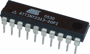
Extract IC ATtiny2313 Code from MCU ATtiny2313’s flash memory, recover heximal to new MCU ATtiny2313 after crack master microcontroller ATtiny2313;
- High Performance, Low Power AVR® 8-Bit Microcontroller
- Advanced RISC Architecture
– 120 Powerful Instructions – Most Single Clock Cycle Execution
– 32 x 8 General Purpose Working Registers
– Fully Static Operation
– Up to 20 MIPS Throughput at 20 MHz
Data and Non-volatile Program and Data Memories
– 2/4K Bytes of In-System Self Programmable Flash
- Endurance 10,000 Write/Erase Cycles
– 128/256 Bytes In-System Programmable EEPROM
- Endurance: 100,000 Write/Erase Cycles
– 128/256 Bytes Internal SRAM when reading chip attiny25v software
– Programming Lock for Flash Program and EEPROM Data Security
Peripheral Features
– One 8-bit Timer/Counter with Separate Prescaler and Compare Mode
– One 16-bit Timer/Counter with Separate Prescaler, Compare and Capture Modes
– Four PWM Channels
– On-chip Analog Comparator
– Programmable Watchdog Timer with On-chip Oscillator
– USI – Universal Serial Interface
– Full Duplex USART
Special Microcontroller Features
– debugWIRE On-chip Debugging
– In-System Programmable via SPI Port
– External and Internal Interrupt Sources
– Low-power Idle, Power-down, and Standby Modes
– Enhanced Power-on Reset Circuit if Extract read microcontroller attiny85 flash
– Programmable Brown-out Detection Circuit
– Internal Calibrated Oscillator
I/O and Packages
– 18 Programmable I/O Lines
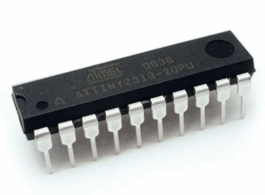
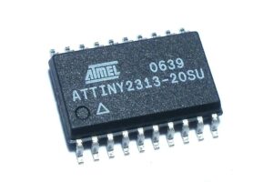
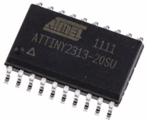
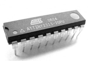
– 20-pin PDIP, 20-pin SOIC, 20-pad MLF/VQFN
Operating Voltage
– 1.8 – 5.5V
Speed Grades
– 0 – 4 MHz @ 1.8 – 5.5V
– 0 – 10 MHz @ 2.7 – 5.5V
– 0 – 20 MHz @ 4.5 – 5.5V
Industrial Temperature Range: -40°C to +85°C
Low Power Consumption
In-System
Programmable Flash
– Active Mode
- 190 µA at 1.8V and 1MHz
– Idle Mode
- 24 µA at 1.8V and 1MHz
– Power-down Mode
- 0.1 µA at 1.8V and +25°C
- Port A is a 3-bit bi-directional I/O port with internal pull-up resistors (selected for each bit). The Port A output buffers have symmetrical drive characteristics with both high sink and source capability, except PA2 which has the RESET capability.
- To use pin PA2 as I/O pin, instead of RESET pin, program (“0”) RSTDISBL fuse. As inputs, Port A pins that are externally pulled low will source current if the pull-up resistors are activated. The Port A pins are tri-stated when a reset condition becomes active, even if the clock is not running.
The difficulty lies not only in bypassing the secured firmware protection but also in safely reading the flash, EEPROM, or configuration bytes without damaging or corrupting the chip. Improper handling during the hack or readout attempt may permanently destroy the stored source code or render the device unusable. Our controlled extraction technique focuses on stability, repeatability, and precision, ensuring that the final dump, archive, or recovered file data is accurate and functional.
Why is this service meaningful? Because many companies rely on legacy systems where firmware cannot be recreated from scratch. By helping clients open, extract, and recover the original program, we enable continued manufacturing, repair support, compatibility upgrades, or deeper engineering analysis. Whether for failure investigation, modernization, or secure archival purposes, retrieving the ATtiny2313 firmware can protect investments, reduce downtime, and ensure long-term product life cycle continuity.
Our goal is simple: transform locked code into accessible engineering value — safely, efficiently, and professionally.