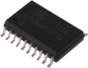
Extract Chip ATtiny4313A Code from its flash memory after unlock microcontroller attiny4313a security fuse bit and recover firmware of mcu attiny4313a heximal same as original functions;

The ATtiny2313A/4313 provides the following features: 2/4K bytes of In-System Programmable Flash, 128/256 bytes EEPROM, 128/256 bytes SRAM, 18 general purpose I/O lines, 32 general purpose working registers, a single-wire Interface for On-chip Debugging, two flexible Timer/Counters with compare modes, internal and external interrupts, a serial programmable USART, Universal Serial Interface with Start Condition Detector, a programmable Watchdog Timer with internal Oscillator, and three software selectable power saving modes.
The Idle mode stops the CPU while allowing the SRAM, Timer/Counters, and interrupt system to continue functioning. The Power-down mode saves the register contents but freezes the Oscillator, disabling all other chip functions until the next interrupt or hardware reset.
In Standby mode, the crystal/resonator Oscillator is running while the rest of the device is sleeping. This allows very fast start-up combined with low-power consumption. The device is manufactured using Atmel’s high density non-volatile memory technology.
The On-chip ISP Flash allows the program memory to be reprogrammed In-System through an SPI serial interface, or by a conventional non-volatile memory programmer.
By combining an 8-bit RISC CPU with In-System Self-Programmable Flash on a monolithic chip, the Atmel ATtiny2313A/4313 is a powerful microcontroller that provides a highly flexible and cost effective solution to many embedded control applications.
The ATtiny2313A/4313 AVR is supported with a full suite of program and system development tools including: C Compilers, Macro Assemblers, Program Debugger/Simulators, In-Circuit Emulators, and Evaluation kits when extracting attiny4313 microcontroller embedded source code.
This documentation contains simple code examples that briefly show how to use various parts of the device. These code examples assume that the part specific header file is included before compilation. Be aware that not all C compiler vendors include bit definitions in the header files and interrupt handling in C is compiler dependent.
Please confirm with the C compiler documentation for more details.

For I/O Registers located in the extended I/O map, “IN”, “OUT”, “SBIS”, “SBIC”, “CBI”, and “SBI” instructions must be replaced with instructions that allow access to extended I/O. Typically, this means “LDS” and “STS” combined with “SBRS”, “SBRC”, “SBR”, and “CBR”.
Note that not all AVR devices include an extended I/O map.
- For compatibility with future devices, reserved bits should be written to zero if accessed. Reserved I/O memory addresses should never be written.
- I/O Registers within the address range 0x00 – 0x1F are directly bit-accessible using the SBI and CBI instructions. In these registers, the value of single bits can be checked by using the SBIS and SBIC instructions.
- Some of the status flags are cleared by writing a logical one to them. Note that, unlike most other AVRs, the CBI and SBI instructions will only operate on the specified bit, and can therefore be used on registers containing such status flags.
- The CBI and SBI instructions work with registers 0x00 to 0x1F only;
- When using the I/O specific commands IN and OUT, the I/O addresses 0x00 – 0x3F must be used. When addressing I/O
Registers as data space using LD and ST instructions, 0x20 must be added to these addresses.

