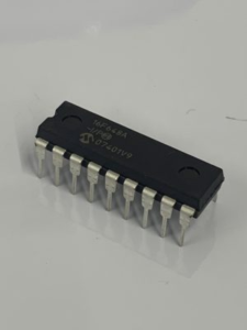
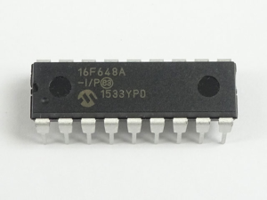
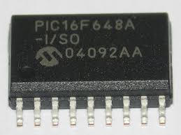
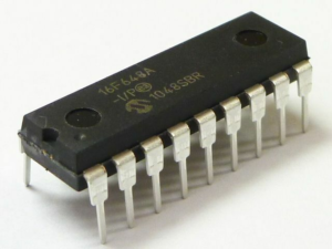
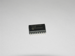
The PIC16F648A is a versatile and highly popular member of the 8-bit microcontroller family, frequently lauded for its generous 4KB flash program memory and its internal oscillator which saves valuable board space. This MCU is widely deployed in various high-precision industries, ranging from automotive aftermarket modules and smart home lighting controllers to specialized industrial timers and security alarm systems. Its architecture includes a built-in comparator and a flexible EEPROM for storing non-volatile user data. Because these devices often house the core operational logic of a commercial product, they are typically shipped as a secured or locked chip. This hardware-level protection is a critical security measure intended to keep the internal firmware an encrypted secret, preventing unauthorized parties from performing a simple extract of the binary file and safeguarding the manufacturer’s R&D investment.
The STATUS register contains the arithmetic status of the ALU, the RESET status and the bank select bits for data memory. The STATUS register can be the destination for any instruction, as with any other register. If the STATUS register is the destination for an instruction that affects the Z, DC, or C bits, then the write to these three bits is disabled. These bits are set or cleared according to the device logic. Furthermore, the TO and PD bits are not writable, therefore, the result of an instruction with the STATUS register as destination may be different than intended. For example, CLRF STATUS will clear the upper three bits and set the Z bit. This leaves the STATUS register as 000u u1uu (where u = unchanged).
It is recommended, therefore, that only BCF, BSF, SWAPF and MOVWF instructions are used to alter the STATUS register, because these instructions do not affect the Z, C, or DC bits from the STATUS register. For other instructions not affecting any status bits, see the “Instruction Set Summary.” The OPTION_REG register is a readable and writable register, which contains various control bits to configure the TMR0 prescaler/WDT postscaler (single assignable register known also as the prescaler), the External INT Interrupt, TMR0 and the weak pull-ups on PORTB.
The INTCON register is a readable and writable register, which contains various enable and flag bits for the TMR0 register overflow, RB Port change and External RB0/INT pin interrupts. The Power Control (PCON) register contains flag bits to allow differentiation between a Power-on Reset (POR), a Brown-out Reset (BOR), a Watchdog Reset (WDT) and an external MCLR Reset. The program counter (PC) is 13 bits wide. The low byte comes from the PCL register, which is a readable and writable register. The upper bits (PC<12:8>) are not readable, but are indirectly writable through the PCLATH register. On any RESET, the upper bits of the PC will be cleared. Figure 2-4 shows the two situations for the loading of the PC. The upper example in the figure shows how the PC is loaded on a write to PCL (PCLATH<4:0> → PCH). The lower example in the figure shows how the PC is loaded during aCALL orGOTO instruction (PCLATH<4:3> → PCH).
Navigating the technical landscape to Copy Microcontroller PIC16F648A Binary data from a device with active “Code Protection” requires a sophisticated level of hardware-based reverse engineering. When an MCU is protected, the internal logic is hardwired to return a null dump or even trigger a self-destruct erase of the memory if it detects a standard attempt to open or hack the program gate. The primary difficulty lies in the fact that you must stabilize the microprocessor at a physical level where the locked state can be bypassed without damaging the underlying data archive. To successfully recover the heximal file, specialists must employ non-invasive or semi-invasive methods to restore visibility to the flash cells. This allows for a clean firmware extract, enabling the creation of a perfect binary dump that effectively pulls the source code logic out of its secured environment into a manageable digital archive.
The motivation to open a protected chip and recover its contents is usually driven by the necessity of industrial longevity and the “Right to Repair.” In many technical fields, a specific microcontroller might be the only surviving copy of a machine’s logic, especially if the original source code was lost due to corporate turnover or a failed server migration years ago. If the PIC16F648A within a vital piece of factory equipment fails, the ability to extract the program from a functional unit is the only way to restore the system. By choosing to reverse engineering the protected MCU, engineers can recover the essential binary and dump it into a new file. This proactive step prevents the total loss of capital-intensive machinery, allowing for the restore of operations by cloning the firmware and EEPROM parameters onto a fresh microprocessor.
For professional clients, the benefits of a successful Copy Microcontroller PIC16F648A Binary service are both immediate and strategic. By securing a verified binary dump of a secured chip, businesses can perform comprehensive security audits on their own encrypted hardware to ensure it is resilient against malicious actors. Furthermore, it allows for the recovery of unique configuration data stored in the EEPROM, which is often the difference between a working machine and an expensive piece of scrap. This service transforms a locked microprocessor into a transparent and recoverable asset, providing a definitive archive of the device’s logic. Whether the goal is to restore a legacy production line, recover lost source code, or create a permanent backup file for an aging MCU, our specialized ability to extract and reverse engineering these chips ensures your technological future is never held hostage by a secured silicon wall.