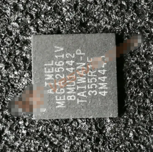
Copy MCU ATmega2561V EEPROM from flash and EEPROM memory refers to a specialized process for retrieving critical binary and heximal data from a secured, protected, or even locked ATmega2561V MCU. This low-power variant of the ATmega2561 combines a high-performance 8-bit AVR microprocessor core with large flash capacity, substantial EEPROM, and flexible memory addressing. In many embedded systems, the internal firmware, runtime program, and configuration file are intentionally restricted to prevent unauthorized access. When official documentation or source code is unavailable, controlled readout becomes the only viable path to preserve functionality.
This documentation contains simple code examples that briefly show how to use various parts of the device. Be aware that not all C compiler vendors include bit definitions in the header files and interrupt handling in C is compiler dependent. Please confirm with the C compiler documentation for more details. These code examples assume that the part specific header file is included before compilation. For I/O registers located in extended I/O map, “IN”, “OUT”, “SBIS”, “SBIC”, “CBI”, and “SBI” instructions must be replaced with instructions that allow access to extended I/O. Typically “LDS” and “STS” combined with “SBRS”, “SBRC”, “SBR”, and “CBR”.
In real projects, Copy MCU ATmega2561V EEPROM from flash and EEPROM memory is not about casual hack behavior, but about structured reverse engineering and professional extract workflows. The goal is to recover meaningful data from non-volatile memory, assemble it into a verified dump, and organize it as a usable archive. Because protection bits and security fuses are designed to resist simple attempts to open or copy content, engineers must work carefully to avoid data loss. Each step prioritizes integrity, ensuring that recovered firmware and parameters accurately reflect the original chip state.
The ATmega2561V is widely deployed in industrial controllers, smart instrumentation, energy management devices, transportation electronics, and communication equipment. Its low-voltage operation and extensive peripheral set make it suitable for long-life products where reliability matters more than raw performance. Over time, manufacturers may discontinue hardware, suppliers may disappear, or maintenance teams may inherit systems with no backups. In such cases, the ability to restore operational data from EEPROM and flash becomes essential for sustaining production lines, repairing field units, or duplicating legacy boards without redesign.
This section discusses the AVR core architecture in general. The main function of the CPU core is to ensure correct program execution. The CPU must therefore be able to access memories, perform calculations, control peripherals, and handle interrupts.
In order to maximize performance and parallelism, the AVR uses a Harvard architecture – with separate memories and buses for program and data. Instructions in the program memory are executed with a single level pipelining. While one instruction is being executed, the next instruction is pre-fetched from the program memory. This concept enables instructions to be executed in every clock cycle. The program memory is In-System Reprogrammable Flash memory. The fast-access Register File contains 32 x 8-bit general purpose working registers with a single clock cycle access time.

This allows single-cycle Arithmetic Logic Unit (ALU) operation. In a typical ALU operation, two operands are output from the Register File, the operation is executed, and the result is stored back in the Register File – in one clock cycle.
Six of the 32 registers can be used as three 16-bit indirect address register pointers for
Data Space addressing – enabling efficient address calculations. One of the these address pointers can also be used as an address pointer for look up tables in Flash program memory. These added function registers are the 16-bit X-, Y-, and Z-register, described later in this section.
The ALU supports arithmetic and logic operations between registers or between a constant and a register. Single register operations can also be executed in the ALU. After an arithmetic operation, the Status Register is updated to reflect information about the result of the operation.
Program flow is provided by conditional and unconditional jump and call instructions, able to directly address the whole address space. Most AVR instructions have a single 16-bit word format. Every program memory address contains a 16- or 32-bit instruction.
Program Flash memory space is divided in two sections, the Boot Program section and the Application Program section. Both sections have dedicated Lock bits for write and read/write protection. The SPM instruction that writes into the Application Flash memory section must reside in the Boot Program section.
Breaking through encrypted or secured protections presents technical and procedural challenges. Incorrect handling can permanently erase valuable program data or corrupt calibration values stored in EEPROM. This is why detailed methods are never casually disclosed. From a client perspective, however, the meaning is clear: successful recovery protects intellectual assets, reduces redevelopment cost, shortens downtime, and enables compliant duplication when legally permitted. By transforming inaccessible memory into a structured archive, Copy MCU ATmega2561V EEPROM from flash and EEPROM memory delivers continuity, risk reduction, and long-term value for complex embedded products.