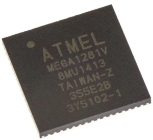
Copy Chip ATmega1281V Binary from its flash and eeprom memory, the secured flash and eeprom memory of MCU ATmega1281V can be cracked by focus ion beam technique, and then recover the embedded binary file from microcontroller atmega1281v;
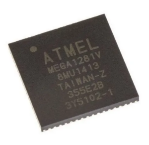
Copying the ATmega1281V binary from flash and EEPROM memory is a specialized technical service focused on obtaining a complete and reliable firmware image from a secured microcontroller. The ATmega1281V is a low-power AVR MCU designed for extended temperature and voltage ranges, combining an efficient 8-bit microprocessor core with large on-chip flash and non-volatile EEPROM resources. These characteristics make it a popular chip for long-life embedded products where stability and data retention are critical.
The device provides up to 128 KB of program flash, multiple communication interfaces, and flexible peripheral control, allowing engineers to store complex program logic, configuration data, and calibration values inside protected memory regions. In many commercial designs, the internal firmware and supporting files are intentionally locked or encrypted to prevent unauthorized access. While this protection is essential for intellectual property, it can become a challenge when products reach maintenance or upgrade stages.
The ATmega1281 is a low-power CMOS 8-bit microcontroller based on the AVR enhanced RISC architecture. By executing powerful instructions in a single clock cycle, the ATmega640/1280/1281/2560/2561 achieves throughputs approaching 1 MIPS per MHz allowing the system designer to optimize power consumption versus processing speed.
The AVR core combines a rich instruction set with 32 general purpose working registers. All the 32 registers are directly connected to the Arithmetic Logic Unit (ALU), allowing two independent registers to be accessed in one single instruction executed in one clock cycle.
The resulting architecture is more code efficient while achieving throughputs up to ten times faster than conventional CISC microcontrollers.
In real projects, clients may need to extract or recover the original binary or heximal image from an ATmega1281V. This requirement often arises when the original source code is lost, when a supplier is no longer available, or when legacy equipment must be cloned for continued production. In such cases, carefully copying the contents of flash and EEPROM into a structured dump or verified archive is the most practical way to restore control over the embedded system.
The main difficulty lies in dealing with protection mechanisms that block standard readout paths. Any improper attempt to open the memory can trigger data loss or permanent lockout. A simplistic hack approach risks corrupting critical memory areas, rendering the MCU unusable. Professional reverse engineering therefore emphasizes non-destructive analysis, consistency checks, and validation of extracted data rather than aggressive intervention. The goal is to obtain an accurate firmware image while preserving the integrity of the original memory.
The ATmega640/1280/1281/2560/2561 provides the following features: 64K/128K/256K bytes of In-System Programmable Flash with Read-While-Write capabilities, 4K bytes EEPROM, 8K bytes SRAM, 54/86 general purpose I/O lines, 32 general purpose working registers.
Real Time Counter (RTC), six flexible Timer/Counters with compare modes and PWM, 4 USARTs, a byte oriented 2-wire Serial Interface, a 16-channel, 10-bit ADC with optional differential input stage with programmable gain, programmable Watchdog Timer with Internal Oscillator, an SPI serial port, IEEE std. 1149.1 compliant JTAG test interface.
Also used for accessing the On-chip Debug system and programming and six software selectable power saving modes. The Idle mode stops the CPU while allowing the SRAM, Timer/Counters, SPI port, and interrupt system to continue functioning.
The Power-down mode saves the register contents but freezes the Oscillator, disabling all other chip functions until the next interrupt or Hardware Reset. In Power-save mode, the asynchronous timer continues to run, allowing the user to maintain a timer base while the rest of the device is sleeping.
The ADC Noise Reduction mode stops the CPU and all I/O modules except Asynchronous Timer and ADC, to minimize switching noise during ADC conversions. In Standby mode, the Crystal/Resonator Oscillator is running while the rest of the device is sleeping. This allows very fast start-up combined with low power consumption. In Extended Standby mode, both the main Oscillator and the Asynchronous Timer continue to run.
ATmega1281V microcontrollers are widely deployed in industrial automation, energy management systems, communication modules, transportation electronics, and custom control units. In these environments, copying the internal program is not about infringement, but about continuity. A clean firmware archive allows companies to replicate hardware, migrate designs to newer platforms, perform failure analysis, and ensure long-term product support.
Ultimately, copying an ATmega1281V binary from flash and EEPROM memory transforms a protected MCU into a manageable asset. For clients, this process reduces redevelopment costs, minimizes downtime, and safeguards years of embedded development by turning inaccessible firmware into usable, well-documented data.