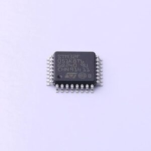
ARM CPU STM32F051K8 Microprocessor Source Code Extraction is for the purpose of restore flash heximal from microcontroller stm32f051k8 after unlock stm chip stm32f051k8 flash memory;
An ARM SW-DP interface is provided to allow a serial wire debugging tool to be connected to the MCU.
- PC13, PC14 and PC15 are supplied through the power switch. Since the switch only sinks a limited amount of current (3 mA), the use of GPIOs PC13 to PC15 in output mode is limited:
- The speed should not exceed 2 MHz with a maximum load of 30 pF.
- These GPIOs must not be used as current sources (e.g. to drive an LED).
- After the first RTC domain power-up, PC13, PC14 and PC15 operate as GPIOs. Their function then depends on the content of the RTC registers which are not reset by the system reset. For details on how to manage these GPIOs, refer to the RTC domain and RTC register descriptions in the reference manual.
- Available on STM32F070C6/F6 devices only.
- TIM15, I2C2, WKUP4, WKUP5, WKUP6, WKUP7, SPI2, USART3 and USART4 are available on STM32F070CB/RB devices only.
- On STM32F070C6/F6 devices, pin pair PA11/12 can be remapped instead of pin pair PA9/10 using SYSCFG_CFGR1 register.
- After reset, these pins are configured as SWDIO and SWCLK alternate functions, and the internal pull-up on the SWDIO pin and the internal pull-down on the SWCLK pin are activated.